
Loading IDSPS Consortium
Loading IDSPS Consortium
India’s next major leap into AI will be shaped by advanced 3D chiplet architectures and technologies, an evolution built on decades of innovations. The 3D Glass Chiplet Package, shown in Figure 1, is proposed as a national test vehicle to advance and integrate each of the technologies from each of the 8 national centres into one national test vehicle.
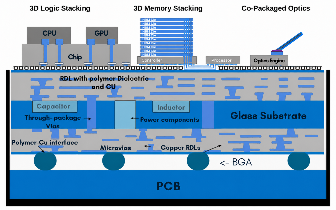
Figure 1: 3D Glass Chiplet Package National Test Vehicle
The foundations of this technology trace back to the pioneering work of Prof. Rao Tummala and his IBM team in the 1980s, who developed the original 2.5D-like multichip module. As shown earlier, this module contained 100–144 small, high-yield chips flip-chip assembled onto a large 127 mm LTCC substrate comprising 61 layers of glass-ceramic-copper. In the modern era, this concept has evolved through organic packages and, more recently, silicon-interposer-based 2.5D solutions introduced by Xilinx and TSMC around 2009. These technologies filled the space between traditional 2D packaging and true 3D stacking, hence the term 2.5D.
As transistor scaling slows and large monolithic SoCs face challenges in yield, design complexity, and cost, the industry has steadily shifted toward modular architectures combining 2.5D and 3D chiplets. This chiplet revolution allows building extremely high transistor-count systems with higher compute performance, lower power consumption, and lower cost compared to previous approaches in the IDSPS Advanced Packaging Program.
To position India as a global leader and a true product nation, it must build deep expertise and infrastructure across eight strategic technologies, shown in Figure 2. These areas, referred to as Strategic Research Areas (SRAs), each encompass multiple high-impact research themes. Together, they form the foundation for establishing eight Industry Co-Development Technology Centres (ICCs), one dedicated to each SRA and a system integration center at IIT Gandhinagar.
These ICCs will work in partnership with leading global companies to design, develop, and demonstrate next-generation, industry-ready technologies. IIT Gandhinagar will serve as the central hub (N-APRC), where advances from all eight centres will be integrated through a pilot line to build advanced, manufacturable system-in-package prototypes. Each ICC will operate its own industry consortium, developing technologies for real industrial test vehicles such as 3D chiplet-integrated packages, thereby accelerating India’s capability for world-class semiconductor productization.
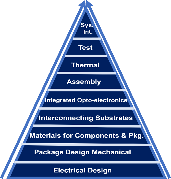
Figure 2: Advanced Packaging requires 8 Strategic Foundational Technologies.
Figure 3 illustrates how innovations from all eight centres will converge at IITGN to create next-generation advanced packages.
Eight ICCs working with N-APRC at IITGN to create next-generation advanced packages.
Figure 3: Advanced Packaging Hub @ IIT GN Converging 8 Strategic Technologies